10 nanometer lines fabricated by electron beam lithography(EBL)
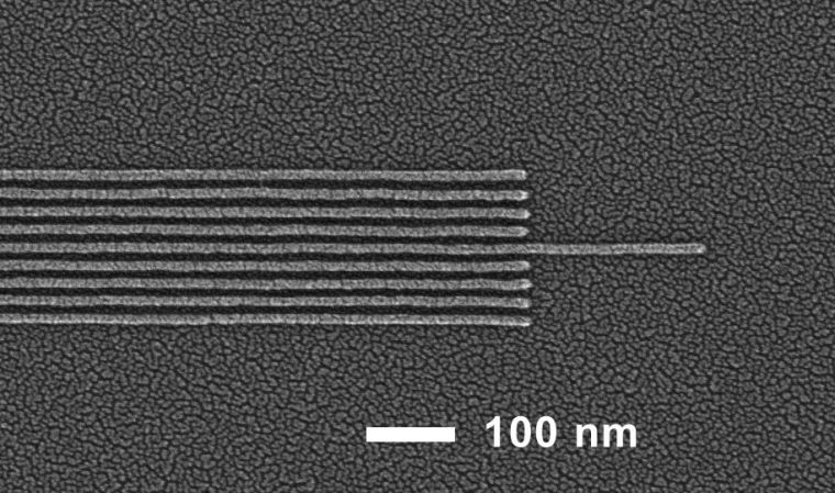
This picture shows an SEM image of a linear grating with ~10 nm lines and a pitch of ~20 nm. The exposure was in ~30nm thick PMMA on a Si substrate where a relatively high dose was used to crosslink the PMMA, rather than using the PMMA as a conventional positive resist. After development, the sample was sputter coated with ~1nm of AuPd. The image was fabricated by Dr Ou in University of Southampton and featured on JC Nabity lithography website.
Nanofabrication on a human hair
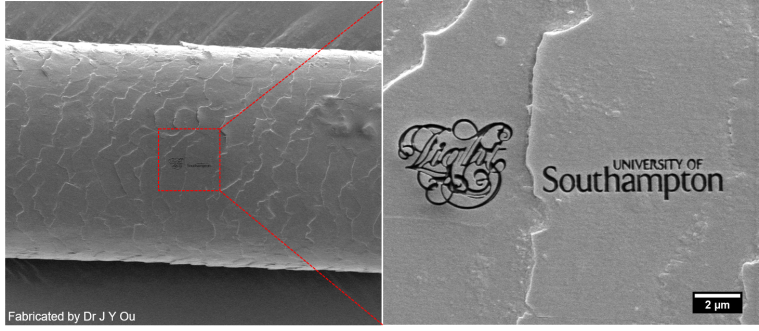
The SEM images show the logos of the Optoelectronic Research Centre and the University of Southampton milled on top of a human hair by FIB. The minimum feature is ~70 nm which is 1000 times smaller than the diameter of a human hair. It is a great example of the nanotechnology and has been demonstrated in several outreach events.
Low Vacuum(1 torr) EBL for non-conductive sample(LiNbO3)
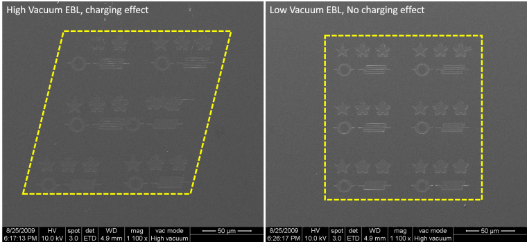

There were no distortion of the patterns on LiNbO3 substrate by using low-vacuum lithography with charging reduction by gaseous process. Moreover, the dots array of 50nm diameter and 200nm pitch has been fabricated. The nanostructure on non-conducted materials can be easily realised by low-vacuum lithography without any additional processes.
Low energy EBL for fast exposure and reduced proximity effect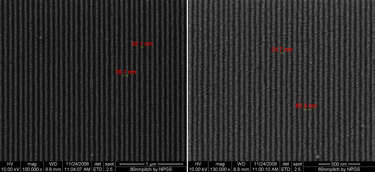
The low-energy EBL has been utilised for exposing nanostructures using FEI Inspect F equipped with JC Nabity lithography system. The resolution achieved with low-energy electrons (2 kV) is found to be about 25 nm for dense lines with pitch of 60nm. The critical exposure dosage is an order of magnitude less then the dosage of the conventional 50kV EBL.
Surface acoustic wave device -undergraduate project
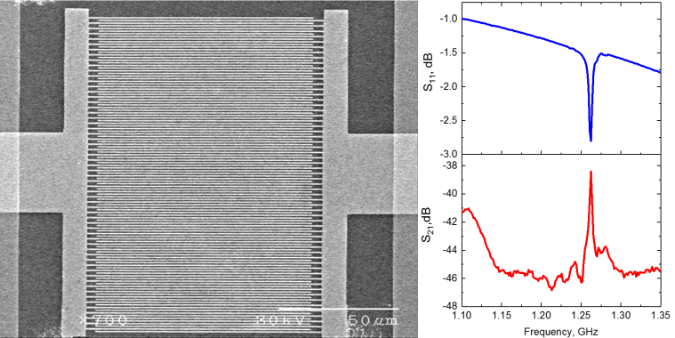
Two surface acoustic wave devices(one generator, one receiver) were fabricated on GaAs(100) subtract with a separation distance of 1.6 mm. The measured reflection coefficient S11 and transmission coefficient S21 show clear resonance at 1.26 GHz with Q-factor of 189 driven by 0 dBm input signal.
My early fabrication, surface acoustic wave device -undergraduate project in 2001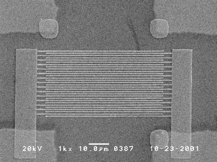
The SEM image shows a 1 GHz operational frequency surface acoustic wave (SAW) generator on GaAs(100) substrate which was fabricated by Dr Ou in National Changhua University of Education, Taiwan using the standard electron beam lithography, metallization, and lift-off process.
More is coming
