Dr Ou has his interest on nanoelectronic devices based on nonvolatile phase change materials from working for the semiconductor company, Macronix International Taiwan, funded project on “phase change memory” in 2007.
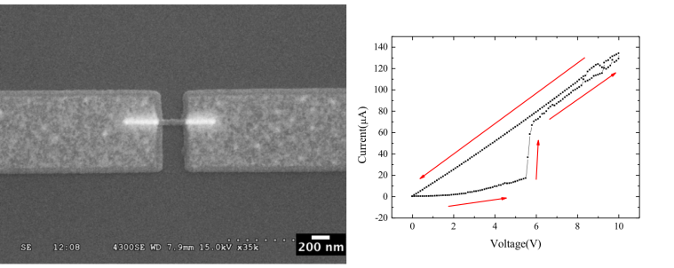
The SEM image with typical I-V characteristic of a lateral Ge2Sb2Te5 device with the dimension of 200nm×80nm×30nm.
After Dr Ou joined Optoelectronic Research Centre, he worked with the world leading team of phase change material, Dr Behrad Gholipour, Dr Chung-Che Huang and Professor Dan Hewak on development of CVD-grown phase change nano-optoelectronic devices.
- Fiber-integrated phase change metasurfaces with switchable group delay dispersion
T. Martins, Y. Cui, B. Gholipour, J. Y. Ou, O. Frazão, and K. F. MacDonald
Adv. Opt. Mater., 2100803 (2021) doi: 10.1002/adom.202100803 – pdf - Germanium antimony lateral nanowire phase change memory by chemical vapor deposition
B. Gholipour, C. C. Huang, J. Y. Ou, D. W. HewakPhysica status solidi (b) 250 (5), 994 (2013) doi:10.1002/pssb.201248515
- Deposition and characterization of CVD-grown Ge-Sb thin film device for phase-change memory application
C. C Huang, B. Gholipour, K. Knight, J. Y. Ou, D. W. Hewak
Advances in OptoElectronics 2012, 840348 (2012) doi:10.1155/2012/840348 - Electrical phase change of CVD-grown Ge-Sb-Te thin film device
C. C. Huang, B. Gholipour, J. Y. Ou, K. J. Knight, and D. W. Hewak
Electron. Lett.47, 288 (2011) doi: 10.1049/el.2010.3276
