Nonclassical Spin-Multiplexing Metasurfaces Enabled Multifunctional Meta-Scope, Small (2024)

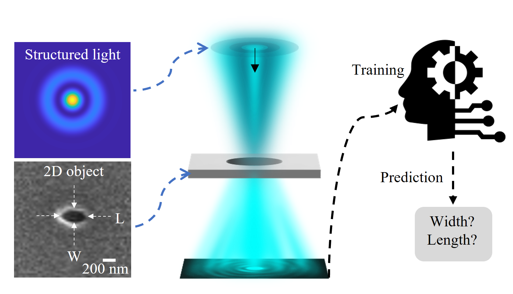
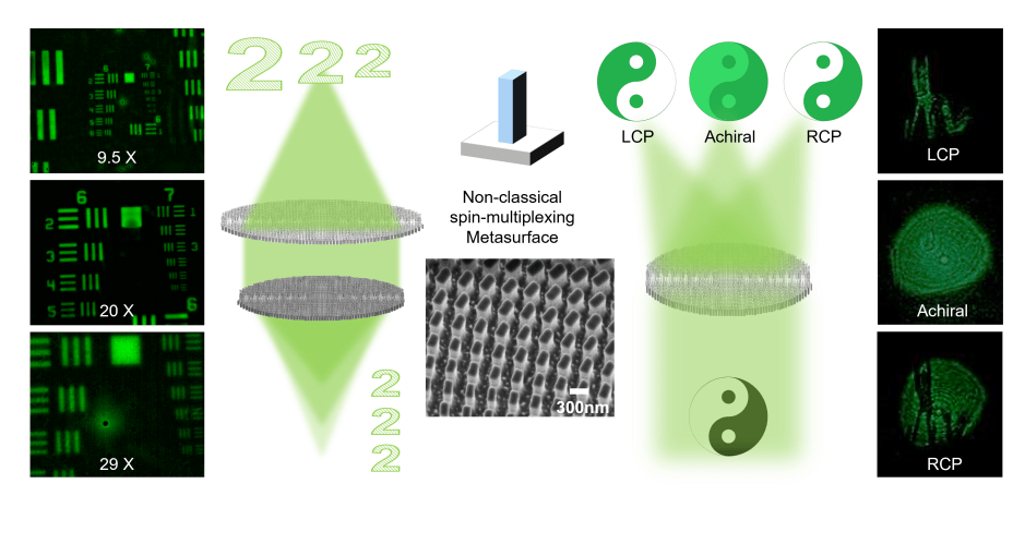
Dielectric metasurfaces have emerged as attractive devices for advanced imaging systems because of their high efficiency, ability of wavefront manipulation, and lightweight. The classical spin-multiplexing metasurfaces can only provide two orthogonal circular polarization channels and require high phase contrast which limits their applications. Here, metasurfaces with arbitrary three independent channels are demonstrated by proposing a nonclassical spin-multiplexing approach exploring the low refractive index meta-atoms. A zoom microscope with on-axis tri-foci and a synchronous achiral-chiral microscope with in-plane tri-foci based on silicon nitride metasurfaces are experimentally demonstrated. Based on the on-axis tri-foci metasurface, singlet zoom imaging with three magnifications and a broadband response (blue to red) based on a single metasurface is first demonstrated. A compact microscope (meta-scope) consisting of two metasurfaces with three magnifications of 9.5, 10, and 29X with diffraction-limited resolutions is further constructed, respectively. Utilizing the in-plane tri-foci metasurface, a singlet microscope with three achiral-chiral channels is demonstrated. It offers a magnification of 53X and a diffraction-limited resolution, enabling simultaneous imaging of an object’s achiral and chiral properties. Our multifunctional metasurfaces and meta-scope approaches could boost the applications in biological imaging and machine vision.

Ref:
Nonclassical spin-multiplexing metasurfaces enabled multifunctional meta-scope
C. Sun, Z. Wang, K. S. Kiang, O. Buchnev, D. Tang, J. Yan, J. Y. Ou*
Small, 2404003 (2024) doi: smll.202404003

Structured light + AI for nanoscale 2D optical metrology, Advanced Science (2024)

Progress in the semiconductor industry relies on the development of increasingly compact devices consisting of complex geometries made from diverse materials. Precise, label-free, and real-time metrology is needed for the characterization and quality control of such structures in both scientific research and industry. However, optical metrology of 2D sub-wavelength structures with nanometer resolution remains a major challenge. Here, a single-shot and label-free optical metrology approach that determines 2D features of nanostructures, is introduced. Accurate experimental measurements with a random statistical error of 18 nm (λ/27) are demonstrated, while simulations suggest that 6 nm (λ/81) may be possible. This is far beyond the diffraction limit that affects conventional metrology. This metrology employs neural network processing of images of the 2D nano-objects interacting with a phase singularity of the incident topologically structured superoscillatory light. A comparison between conventional and topologically structured illuminations shows that the presence of a singularity with a giant phase gradient substantially improves the retrieval of object information in such an optical metrology. This non-invasive nano-metrology opens a range of application opportunities for semiconductor metrology, quality control, and advanced materials characterization.

Ref:
2D super-resolution metrology based on superoscillatory light
Y. Wang*, E. A. Chan, C. Rendón-Barraza, Y. Shen, E. Plum, and J. Y. Ou*
Adv. Science, 2404607 (2024) doi: 10.1002/advs.202404607

Metalens for tunable dual-mode microscope Advanced Optical Materials (2024)

The spiral phase contrast microscope can clearly distinguish the morphological information of the low contrast objects (i.e., biological samples) owing to the isotropic edge-enhancement effect, while the bright field microscope can image the overall morphology of amplitude objects. However, the imaging resolution, magnification, and field of view of conventional spiral phase contrast microscopes based on 4f filtering configuration are limited by the system’s complexity. Here, compact dual-mode microscopes working at near-infrared using the engineered metalens are reported, which can be tuned between the spiral phase contrast imaging and bright field imaging by polarization control. The metalens combines the high-resolution objective lens and polarization-controlled phase filter into a single-layer nanofin array. Two infinity-corrected microscope systems are demonstrated to achieve subwavelength resolution (0.7λ), large magnification (58X), and large field of view (600 × 800 µm). Unstained onion epidermal is imaged by the microscope to show the dual-mode imaging ability of the biological sample. Finally, a singlet dual-mode microscope system is demonstrated to show the edge-detection application for industrial standards. These results can open new opportunities in applications of biological imaging, industrial machine vision, and semiconductor inspection.

Ref:
Near-infrared metalens empowered dual-mode high resolution and large FOV microscope
C. Sun, H. Pi, K. S. Kiang, J. Yan and J. Y. Ou
Adv. Opt. Mater. 12, 2400512 (2024) doi:10.1002/adom.202400512

Tunable optical traps for levitating particles with metalens, Nanophotonics (2024)

Optically levitated multiple nanoparticles have emerged as a platform for studying complex fundamental physics such as non-equilibrium phenomena, quantum entanglement, and light-matter interaction, which could be applied for sensing weak forces and torques with high sensitivity and accuracy. An optical trapping landscape of increased complexity is needed to engineer the interaction between levitated particles beyond the single harmonic trap. However, existing platforms based on spatial light modulators for studying interactions between levitated particles suffered from low efficiency, instability at focal points, the complexity of optical systems, and the scalability for sensing applications. Here, we experimentally demonstrated that a metasurface that forms two diffraction-limited focal points with a high numerical aperture (∼0.9) and high efficiency (31 %) can generate tunable optical potential wells without any intensity fluctuations. A bistable potential and double potential wells were observed in the experiment by varying the focal points’ distance, and two nanoparticles were levitated in double potential wells for hours, which could be used for investigating the levitated particles’ nonlinear dynamics, thermal dynamics, and optical binding. This would pave the way for scaling the number of levitated optomechanical devices or realizing paralleled levitated sensors.

Ref:
Tunable on-chip optical traps for levitating particles based on single-layer metasurface
C. Sun, H. Pi, K. S. Kiang, T. S. Georgescu, J. Y. Ou*, H. Ulbricht, J. Yan*
Nanophotonics (2024) published online DoI:10.1515/nanoph-2023-0873


Picophotonic localization metrology beyond thermal fluctuations Nature Materials(2023)

Despite recent tremendous progress in optical imaging and metrology, there remains a substantial resolution gap between atomic-scale transmission electron microscopy and optical techniques. Is optical imaging and metrology of nanostructures exhibiting Brownian motion possible with such resolution, beyond thermal fluctuations? Here we report on an experiment in which the average position of a nanowire with a thermal oscillation amplitude of ∼150 pm is resolved in single-shot measurements with subatomic precision of 92 pm, using light at a wavelength of λ = 488 nm, providing an example of such sub-Brownian metrology with ∼λ/5,300 precision. To localize the nanowire, we employ a deep-learning analysis of the scattering of topologically structured light, which is highly sensitive to the nanowire’s position. This non-invasive metrology with absolute errors down to a fraction of the typical size of an atom, opens a range of opportunities to study picometre-scale phenomena with light.

Picophotonic localization metrology beyond thermal fluctuations
T. Liu,C-H.Chi, J. Y. Ou,J.Xu,E.A. Chan,K. F. MacDonald and N. I. Zheludev
Nat. Mater. (2023) doi: 10.1038/s41563-023-01543-y